Bruker Nano Surfaces
Bruker Nano Surfaces List of Employees There's an exhaustive list of past and present employees! Get comprehensive information on the number of employees at Bruker Nano Surfaces. You can filter them based on skills, years of employment, job, education, department, and prior employment.
Bruker Nano Surfaces Salaries. You can even request information on how much does Bruker Nano Surfaces pay if you want to. Learn about salaries, pros and cons of working for Bruker Nano Surfaces directly from the past employees.
Find People by Employers You can rekindle an old relationship, reconnect with a long-lost friend, former boss, business acquaintance who might be useful in your new line of work. With our employee database, the possibilities are endless. All you have to do is type in a couple of keywords and we'll bring you the exact information you wanted!
73 Bruker Nano Surfaces employees in database. Find out everything there's to know about Bruker Nano Surfaces employees. We offer you a great deal of unbiased information from the internal database, personal records, and many other details that might be of interest to you.
Bruker Nano Surfaces Employees
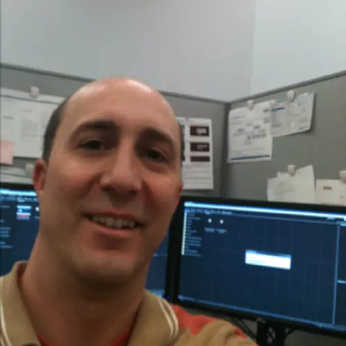
 Mark DeVol
 ManTech International Corporation June 2015 - Present
Bruker Nano Surfaces 2014 - 2015
ManTech 2010 - 2014
Teledyne Brown Engineering 2010 - 2010
Newtec 2005 - 2010
Skills
C#, .NET, ASP.NET, ADO.NET, T-SQL, C++, C, ASP.NET AJAX, WPF, LINQ, Visual Studio, Agile Methodologies, Windows software..., Software Development, Software Design, Object Oriented Design, Database Design, Software Engineering, Microsoft SQL Server, Databases, SSDT, TFS, IIS, XML, VB.NET, HTML, HTTP, Android Development, Eclipse, Java, JavaScript, TCP/IP, UDP, DNS, EDI ANSI X12, FTP, RPC, MTP
Education
The Ohio State University 1979 — 1982
Bachelor of Science (BS), Management Information Systems
New Mexico Military Institute 1977 — 1979
Associate of Science (AS), Business
Bruker Nano Surfaces June 2010 - Present
U.S. Cellular February 2009 - March 2010
Education
Madison Area Technical College 2006 — 2009
Electronics Technology
 Angela Vigorito
 Bruker Nano Surfaces January 2011 - Present
CDEX, Inc August 2008 - February 2009
Lasertel October 2007 - August 2008
United States Postal Service January 2007 - November 2007
Spectra-Physics April 2004 - May 2007
Skills
Manufacturing, Optics, Metrology, Semiconductors, Electronics, R&D, Design of Experiments, Failure Analysis, Lean Manufacturing, Engineering Management, Product Development, Cross-functional Team..., Thin Films
Education
Carrington College-Tucson 2010 — 2011
Medical Insurance Coding Specialist/Coder
VMI September 2014 - Present
Bruker Nano Surfaces November 2012 - July 2014
ON Semiconductor January 2011 - November 2012
ASM August 2004 - August 2010
ASM 2002 - 2004
Skills
Product Management, Product Marketing, Semiconductors, Chinese, Product Life Cycle, Metrology, Product Development, Business Development, Program Management, Key Account Management, Chemical Engineering, MBA, International Business, Management, Business Strategy, R&D, Cross-functional Team...
Education
Thunderbird School of Global Management 2002 — 2003
MBA, International Business
Brigham Young University 1995 — 1999
Bachelor's Degree, Chemical Engineering
 Jeff Kwast
 Bruker Nano Surfaces July 2014 - Present
Bruker Nano Surfaces July 2013 - July 2014
Bruker Nano Surfaces December 2011 - July 2013
Bruker Nano Surfaces March 2008 - December 2011
Veeco Instruments October 2006 - March 2008
Skills
Electronic Circuit..., PCBA Design, OrCAD Capture CIS, Allegro, Control Engineering, Solid Edge, Motor Control, Metrology, Altium Designer, NI TestStand, Labview, FPGA prototyping, Altera, Quartus, Automation, Piezoelectric Actuators, Python, C / C++ / C#, NFPA 70: National..., NFPA 79, IEC 61010-1, IEC 60204-1, SEMI S22, Semiconductors, Manufacturing, Testing, R&D, Matlab, Engineering Management, Product Development, Lean Manufacturing, Product Management, Continuous Improvement, Medical Devices, Product Lifecycle..., Project Management, Product Marketing, Program Management, Process Improvement, Electronics, PCB Design, Visual Basic, Semiconductor Industry, Engineering, Sensors, Atomic Force Microscopy, Piezoelectric, Embedded Systems, AFM
Education
UCSB
Bachelor of Science (B.S.), Electrical and Electronics Engineering
 Ben Hoselton
 Visicon Technologies, Inc April 2014 - Present
Bruker Nano Surfaces February 2012 - July 2012
JumpSport July 2011 - September 2011
Medtronic July 2009 - September 2009
Skills
Microsoft Excel, PowerPoint, Outlook, Windows, Microsoft Word, HTML, Public Speaking, Research, English, Microsoft Office, Teaching, C, Editing, C++, Manufacturing, Matlab, Mechanical Engineering, Solidworks, AFM, Labview, Simulations, Finite Element Analysis, Engineering, AutoCAD, Design of Experiments, Mathematica, SolidWorks, LabVIEW, R&D
Education
Cornell University 2012 — 2013
Master of Engineering (MEng), Engineering Physics/Applied Physics
California Polytechnic State University-San Luis Obispo 2007 — 2011
Bachelor of Science (BS), Mechanical Engineering
Swinburne University of Technology 2010 — 2010
Mechanical Engineering
Agoura High School
 Igor Titushkin
 Bruker Nano Surfaces May 2013 - Present
NanoInk, Inc. March 2010 - February 2013
University of Illinois at Chicago August 2006 - November 2010
University of Illinois at Chicago October 2003 - August 2006
Max Planck Institute for Metals Research September 2002 - September 2003
Center for Biomaterials, Moscow September 1996 - July 2002
Skills
Nanotechnology, AFM, Characterization, Customer Support, Biomaterials, Microscopy, Assay Development, Cellular Assays, Stem Cells, Bioengineering, Scanning Electron..., Confocal Microscopy
Education
Moscow Institute of Physics and Technology (State University) (MIPT) 1999 — 2002
PhD, Biophysics
Moscow Institute of Physics and Technology (State University) (MIPT) 1993 — 1999
MS, Physics and Engineering
 Jesse Andersen
 IM Flash April 2015 - Present
United States Postal Service January 2015 - April 2015
Bruker Nano Surfaces February 2013 - December 2014
Bruker Nano Surfaces October 2012 - February 2013
Allan Hancock College January 2008 - July 2010
Skills
Physics, Solidworks, Mathematica, Statistics, Chemistry, Machining, Experimental Physics, Matlab, Engineering, Optics, Labview, Simulations, Numerical Analysis, Science, Materials Science, Applied Mathematics, Nanotechnology, Mathematics, Problem Solving, Technical Writing, Technical Documentation, Failure Analysis, Data Analysis, Data Collection, Technical Presentations, Microsoft Access, Calibration, SolidWorks
Education
University of california Santa Barbara 2010 — 2012
Bachelor of Applied Science (B.A.Sc.), Physics
Allan Hancock College 2007 — 2010
Associate of Science (A.S.), Mathematics
John F. Kennedy High School 1992 — 2006
Abitur and High School Diploma
 Sandip Basu
 Bruker Nano Surfaces February 2015 - Present
GT Advanced Technologies March 2014 - December 2014
Agilent Technologies August 2011 - March 2014
Texas A&M University December 2009 - August 2011
Rutgers University September 2008 - December 2009
Skills
Materials Science, Materials, Spectroscopy, Nanotechnology, AFM, Characterization, Powder X-ray Diffraction, Thin Films, Scanning Electron..., Nanomaterials, Biomaterials, TGA, Chemistry, Physics, R&D, Microscopy, Electron Microscopy, Optical Microscopy, Electrochemistry
Education
Drexel University 2003 — 2008
Ph.D., Materials Science and Engineering
Indian Institute of Technology, Banaras Hindu University 2000 — 2002
M.S., Ceramic Engineering
 Jacob Zander
 Xcel Mechanical Systems, Inc. September 2011 - Present
Bruker Nano Surfaces June 2010 - December 2010
ATK Space Systems, Inc June 2009 - April 2010
W.E. O'Neil Construction June 2006 - September 2008
Skills
Solidworks, Matlab, MIG welding, Arc Welding, Pro Engineer, Mechanical Engineering, Solid Edge, Finite Element Analysis, AutoCAD, Project Engineering, Engineering, Stress Analysis, Machine Design, Fluid Mechanics, Manufacturing, Piping, Construction, Machining, SolidWorks, PTC Creo
Education
California State Polytechnic University-Pomona 2005 — 2011
Bachelor of Science (B.S.), Mechanical Engineering
Monta Vista High School 2001 — 2005
 Sara Tichenor
 Bruker Nano Surfaces June 2014 - Present
Bruker Nano Surfaces April 2011 - June 2014
Bruker Nano, Inc. October 2010 - April 2011
Veeco Instruments March 2009 - January 2011
Veeco Instruments September 2007 - March 2009
Veeco Instruments December 2005 - August 2007
Hitachi High Technologies 2000 - December 2005
EDAX Inc. 1998 - 2000
Kevex January 1997 - October 1997
Skills
Nanotechnology, Product Development, Product Marketing, Product Management, Metrology, Product Launch, Spectroscopy, Cross-functional Team..., Competitive Analysis, Project Management, Strategic Planning, Business Development, Data Analysis, Analysis, Electronics, Marketing Strategy, R&D, CRM, Forecasting
Education
Bates College 1992 — 1996
BA, Geology
 Paul Anzalone
 Bruker-Nano Surfaces March 2012 - Present
Anzalone Design January 2011 - Present
Arizona Citizens Defense League November 2010 - Present
GLHN Architects & Engineers July 2008 - January 2011
Town of Oro Valley June 2007 - July 2008
PRSA 2007 - 2008
Velcro USA, Inc. Consumer Div. November 2002 - March 2007
Raytheon Missile Systems January 2000 - November 2002
Skills
Photoshop, Advertising, Booklets, PowerPoint, Photography, Art Direction, Packaging, InDesign, Newsletters, Adobe Creative Suite, Graphics, Illustration, Brochures, Project Management, Marketing, Visual Communication, QuarkXPress, Corporate Branding, Pre-press, Graphic Design, Adobe Acrobat, Typography, Layout, After Effects, Brand Development, Digital Photography, Illustrator, Image Manipulation, Magazines, Multimedia, Mac, Web Design, Direct Mail, Copywriting, Publications, Flash
Education
Northern Arizona University 1986 — 1993
Salpointe Catholic 1982 — 1986
Bruker Nano Surfaces January 2015 - Present
Grote Industries March 2014 - January 2015
University of Central Florida January 2010 - January 2014
Univeristy of Central Florida August 2004 - December 2009
ERC 1998 - 2004
Skills
Organic Synthesis, Two-photon Microscopy, Mammalian Cell Culture, Cancer Cell Biology, Differential Scanning..., Thermal Analysis, NMR spectroscopy, Fluorescence..., Fluorescence Anisotropy, Microwave Synthesis, Photodynamic Therapy, Apoptosis, Immunofluorescence, Immunohistochemistry, Confocal Laser Scanning..., Lithography, Image Processing, ImageJ, Receptors, Binding Assays, Receptor Binding Assays, Cell Viability Assays, Confocal Microscopy, Spectroscopy, UV/Vis, IR, Purification, NMR, Nanoparticles, Microscopy, Organic Chemistry, Gas Chromatography, Epoxy Resins, Column Chromatography, Experimentation, Assay Development, Fluorescence, Cell Biology, Chemistry, Cell Culture, Fluorescence Microscopy, Polymers, TGA
Education
University of Central Florida 2009 — 2012
Postdoc, Oncology and Cancer Biology, Photodynamic Therapy
University of Central Florida 2004 — 2009
Doctor of Philosophy (Ph.D.), Chemistry
Universidad Simón Bolívar 1998 — 2003
Bachelor's degree, Organic Chemistry
 Teimour Maleki
 Asylum Research, an Oxford Instruments Company August 2015 - Present
Bruker Nano Surfaces April 2014 - June 2015
Bruker Nano, Inc. April 2012 - March 2014
Purdue University October 2010 - April 2012
Purdue University February 2010 - October 2010
Purdue University January 2006 - January 2010
RSA Electronics May 2003 - June 2005
Skills
Microfabrication, Packaging, Implantable devices, FIB, Thin Films, Microscopy, LaTeX, COMSOL, Simulations, Matlab, AFM, Characterization, PCB design, Analog Circuit Design, Sputtering, Raman, Biomedical Engineering, R&D, Scanning Electron..., MEMS, TEM, Signal Processing, Optics, Physics, Clean Rooms, Microfluidics, Microcontrollers, Image Processing, Experimentation, Mathematical Modeling, Labview, Sensors, Medical Devices, Mathematica, Photolithography, Confocal Microscopy, Design of Experiments, Semiconductors, Nanofabrication, Lithography, Spectroscopy, PECVD, Materials Science, Ellipsometry, CVD, Implants, Analog, Powder X-ray Diffraction, Photonics, Nanomaterials
Education
Purdue University 2006 — 2010
Ph.D, Electrical and Computer Engineering
University of Tehran 2000 — 2003
M.Sc, Electrical and Computer Engineering
Amirkabir University of Technology - Tehran Polytechnic 1996 — 2000
B.Sc, Biomedical Engineering
 Thomas Mueller
 Bruker Nano Surfaces November 2013 - Present
Bruker Nano Surfaces October 2010 - November 2013
Veeco Instruments June 2007 - October 2010
Veeco Instruments January 2006 - June 2007
Veeco Instruments January 2004 - January 2006
Skills
Targets, Semiconductors, Nanotechnology, Materials Science, Spectroscopy, R&D, Optics, AFM, Chemistry, Cross-functional Team..., Biotechnology, Scanning Probe..., Metrology, Solar Cells, Semiconductor Industry, Science, Polymers, Product Lifecycle..., Physics, Product Marketing, Analytical Chemistry, Photonics, Instrumentation, Lifesciences, Communication, Product Management, Materials, Optical Microscopy, Microscopy, Product Development, Product Launch, Technology Transfer, Characterization, Commercialization, Competitive Analysis, Nanoparticles, UV/Vis, Physical Chemistry, Raman, IR, Surface, Business Strategy, Nanomaterials, Scanning Electron..., Surface Chemistry, Vacuum, Optoelectronics, MEMS, Life Sciences
Education
Columbia University in the City of New York 2000 — 2003
Postdoctoral Research Fellow, Physical Chemistry
Yale University 1993 — 2000
PhD, Physical Chemistry
Technische Universität Darmstadt 1990 — 1993
Chemistry
Goethe Gymnasium
 Trevor Chitwood
 Bruker Nano Surfaces May 2015 - Present
Owens Harkey Advertising August 2014 - April 2015
Automatit Inc June 2013 - July 2014
FlipSwitch January 2013 - June 2013
StrongMind January 2013 - June 2013
Milea Truck Sales Corporation November 2011 - January 2013
Freeway chevrolet 2003 - 2004
Skills
Google Adwords, Automotive, Account Management, New Business Development, SEM, Digital Marketing, Google Analytics, Email Marketing, Integrated Marketing, Mobile Marketing, Social Media Marketing, Social Media Measurement, Search Advertising, SEO, Social Media, Home Infusion, WordPress, Omniture, Zoho, Basecamp, Photoshop, Analytics, E-commerce, Digital Media
Education
NYU 2012 — 2012
Digital Media Marketing Certificate, Marketing
Arizona State University 2011 — 2013
Bachelor of Arts (BA), Psychology
Central Arizona College 2009 — 2011
Associate of Arts and Sciences (AAS), Manufacturing Engineering
 Thomas (Tom) Fothergill
 Bruker Nano Surfaces September 2015 - Present
Bruker Nano Surfaces July 2015 - September 2015
University of Wisconsin-Madison March 2010 - June 2015
The University of Queensland March 2006 - February 2010
The University of Queensland 2003 - 2006
The University of Queensland January 2002 - December 2002
Skills
Neuroscience, Cell Biology, Molecular Biology, Fluorescence Microscopy, Confocal Microscopy, TIRF Microscopy, Immunohistochemistry, Tissue Culture, Virology, Project Management, Team Leadership, Scientific Writing, Data Analysis, Western Blotting, Science, Cell, Research, Axon Guidance, Cytoskeleton, Histology, Immunology, Cell Culture, Cancer Research, Protein Purification, Antibodies, Microscopy, Mammalian Neuron Culture, Animal Models, Immunofluorescence, Flow Cytometry, Teaching, Group Presentations, Marketing Management, Statistics, Protein Expression, Molecular Cloning, PCR, Transfection, Life Sciences, Genetics, Biochemistry, Endoplasmic Reticulum, Bioinformatics, Graphic Design, Technical Diving, Photography, Computer Maintenance, qPCR, Laboratory, In Vivo
Education
The University of Queensland 2002 — 2006
PhD, Molecular Bioscience
The University of Queensland 2001 — 2001
BSc(Hons), Virology, Class I
The University of Queensland 1998 — 2000
BSc, Microbiology, Biochemistry
 David Douglass
 Las Cumbres Observatory June 2014 - Present
Software Engineering 2013 - June 2014
Bruker Nano Surfaces 2005 - 2013
Northrop Grumman Corporation / Mission Systems / TSD 2004 - 2005
Veeco / Digital Instruments 2002 - 2004
Polycom 2000 - 2002
Hewlett-Packard / Transoft Networks 2000 - 2000
eFax.com 1997 - 2000
Digital Media International 1994 - 1997
Skills
Software Development, C++, Debugging, C, C#, Software Architectural..., Java, Embedded Systems, Refactoring, Scrum, Object Oriented Design, Design Patterns, MFC, Visual Studio, Device Drivers, Programming, SOA, Windows, STL, Win32 API, Perforce, Multithreading, OOP, Software Engineering, DirectShow, R&D, Embedded Software, Agile Methodologies, UML, Linux, Boost, ATL, ATM networks, TCP/IP, CVS, Instrument Control, Visual C++, System Architecture, Algorithms, COM, DirectX, JTAG, Serena Business Manager, x86 Assembly, PowerPC, MIPS, WinDDK
Education
Bucknell University
Bachelor of Science (BS), Computer Engineering
Rutgers, The State University of New Jersey-New Brunswick
Computer Science
 Johannes Plambeck
 Newmark Grubb Knight Frank June 2014 - Present
Cornell University August 2013 - June 2014
Cornell Olin Library September 2012 - June 2014
Cornell Division of Nutritional Sciences March 2013 - April 2014
GIS June 2013 - August 2013
Transportation Alternatives May 2013 - August 2013
Cornell Program on Applied Demographics September 2012 - December 2012
U.S. Department of State May 2012 - September 2012
Bruker Nano Surfaces January 2012 - May 2012
U.S. Department of State September 2011 - December 2011
Skills
ArcGIS, GIS, Python, Microsoft Office, Data Analysis, Analysis, Stata, Research, Access, Statistics, Microsoft Excel, SPSS, Policy Analysis, Spatial Analysis, PowerPoint, Public Speaking, Editing, Policy, Economics, Statistical Modeling, VBA, Matlab, Customer Service, Microsoft Word, Teaching, SAP, Economic Research, Outlook, GAMS, IMPLAN
Education
Cornell University 2012 — 2014
M.S., Regional Science, Demography minor
Ventura College 2010 — 2012
ESRI GIS Certification, Geographic Information Science and Cartography, 3.8
University of California, Davis 2006 — 2010
B.A., Economics, International Relations
The University of Göttingen 2008 — 2009
B.A., International Economics, Political Science
 Carl Ebeling
 Bruker Nano Surfaces 2015 - Present
Skills
Physics, Optics, Spectroscopy, Biomedical Engineering, Mathematica, Nanotechnology, Characterization, Mathematical Modeling, Image Processing, Microscopy, Science, Lifesciences, Digital Imaging, Fluorescence Microscopy, Optical Microscopy, Chemistry, Labview, Photonics, Confocal Microscopy, Data Analysis, Molecular Biology, LabVIEW
Education
University of Utah 2008 — 2013
Doctor of Philosophy (Ph.D.)
Carleton College 1999 — 2003
Bachelor of Arts (B.A.)
 Michael Robitaille
 Bruker Nano Surfaces November 2014 - Present
Northeastern University September 2009 - May 2014
Complex & Nonlinear Physics Laboratory June 2007 - July 2009
Clark University Physics Department August 2007 - April 2009
Skills
Analysis, Physics, Mathematical Modeling, Matlab, LaTeX, Statistics, Data Analysis, Research, Solidworks, Mathematica, Abaqus, Science, C++, Linux, Microscopy, Characterization, R, Experimentation, Image Processing, AFM
Education
Northeastern University 2011 — 2014
Doctor of Philosophy (Ph.D.), Bioengineering and Biomedical Engineering
Northeastern University 2009 — 2011
M.S., Mechanical Engineering
Clark University 2005 — 2009
BA, Physics (Highest Honors), Mathematics minor
 William Sarnack-Alley
 Bruker Nano Surfaces December 2014 - Present
B/E Aerospace July 2014 - Present
Paragon Space Development Corporation September 2013 - April 2014
Raytheon Missile Systems 2006 - 2013
Pratt & Whitney 1980 - 1988
Skills
Trade Studies, Radar, Engineering Management, Aerospace, Mechanical Engineering, Earned Value Management, Pro Engineer, Product Design, Problem Solving, Root Cause Analysis, Mechanical Product..., Design for Manufacturing, GD&T, Manufacturing..., Aircraft
Education
University of Miami 1972 — 1976
BSME, Mechanical Engineering
University of Arizona
MSEE, Microelectronic Packaging
 Paul Scagnetti
 Bruker Nano Surfaces 2014 - May 2015
FEI Company 2012 - 2014
FEI Company 2007 - 2012
FEI Company 2003 - 2007
FEI Company 2001 - 2003
Intel Corporation 1998 - 2001
Intel Corporation 1996 - 1998
CoorsTek 1994 - 1996
Skills
P&L Management, Product Marketing, New Business Development, M&A experience, Mergers & Acquisitions, Materials Science, Scanning Electron..., Characterization, Business, Science, Marketing, TEM, SEM, FIB, Change Management, Life Sciences, Marketing Strategy, Analysis, Entrepreneurship, Mergers, New Business Launch, Lifesciences, Semiconductors, Management
Education
Massachusetts Institute of Technology 1990 — 1996
Doctor of Philosophy (Ph.D.), Mechanical Engineering
University of Oregon 1998 — 2000
Master of Business Administration (M.B.A.), Business
Boston University 1990 — 1992
Master's Degree, Mechanical Engineering
Rhode Island School of Design 1986 — 1990
Bachelor's Degree, Industrial and Product Design
 Garrett Valenzuela
 Bruker Nano Surfaces October 2013 - Present
Arizona Athletics July 2012 - May 2013
Nordstrom’s Rack July 2011 - December 2012
Bank of America May 2010 - June 2011
Chase July 2008 - May 2010
Wendtland & Associates CPA September 2007 - May 2008
Skills
Customer Service, Photoshop, Research, Social Media, Public Speaking, Teamwork, Sports Marketing, Graphic Design, Critical Thinking, Problem Solving, Interpersonal Skill, Communication Skills
Education
University of Arizona, Eller College of Management 2010 — 2013
Bachelor of Business Administration (B.B.A.), Business Administration and Management, General
Pima Community College 2007 — 2010
Associate of Science, Business Management
 CJ Rainville
 Bruker Nano Surfaces June 2014 - Present
Sensintel June 2013 - April 2014
BAE Systems March 2012 - June 2013
Various July 2011 - March 2012
Photometrics July 2010 - July 2011
Photometrics January 2008 - March 2010
Photometrics February 2006 - December 2007
Photometrics March 1994 - January 2006
IBM November 1979 - May 1993
Vermont Educational Television Network June 1975 - November 1979
Skills
Excellent Interpersonal, Troubleshooting, Cost Analysis/Reduction, Process Management, Develop Processes and..., Develop / Maintain..., Data Analysis, New Product Development, ISO 9000 Certification, Staff and Team..., Resolve Software,..., Electronics, Manufacturing, Testing, Electrical Engineering, Imaging, Microsoft Office, Problem Solving, Social Skills, Cost, Sensors, Labview, Product Development, Manufacturing..., Engineering Management, Debugging, Digital Imaging, Design for Manufacturing, Project Management, Program Management, R&D, LabVIEW, Engineering
Education
University of Arizona 1985 — 1990
BSEE, Electrical Engineering
Vermont Technical College 1973 — 1975
ASEE, Electrical Engineering
Custom Control Sensors October 2014 - Present
Rolls-Royce August 2011 - October 2014
UC Santa Barbara September 2010 - June 2011
Bruker Nano Surfaces June 2010 - September 2010
NuVasive September 2009 - June 2010
Veeco Slider Process Equipment September 2009 - May 2010
Skills
Solidworks, Finite Element Analysis, Machining, Labview, Manufacturing, Mechanical Engineering, Microsoft Office, Matlab, Testing, Abaqus, CAD, GD&T, Solid Edge, COSMOS, Data Acquisition, Materials, Tolerance Analysis, Composites, Heat Transfer, Test Fixtures, Cosmos FEA, Design for Manufacturing, Process Improvement, Project Management, Six Sigma, Lean Manufacturing, Statistical Process..., Aerospace, Aerospace Manufacturing, Aerospace Structures, Composite Structures, R&D, Statistical Data..., Engineering, Microsoft Excel, Leadership, Training, Technical Training, Engineering..., Electromechanical..., MEMS Sensors, SolidWorks
Education
University of California, Santa Barbara 2010 — 2011
Master's Degree, Economics
University of California, Santa Barbara 2006 — 2010
Bachelor's Degree, Mechanical Engineering
 David Henz
 Bruker Nano Surfaces October 2014 - Present
Edmund Optics January 2011 - October 2014
The University of Arizona August 2009 - May 2011
Edmund Optics June 2008 - January 2011
Los Alamos National Laboratory January 2007 - May 2008
Los Alamos National Laboratory 2007 - 2007
Skills
Product Management, Optics, Product Development, Engineering Management, SAP, S&OP implementation, Engineering Design, Cross-functional Team..., Product Marketing, Engineering, Leadership, Analysis, Strategy, Simulations
Education
University of Arizona, College of Optical Sciences 2006 — 2008
MS, Optical Sciences
University of Arizona, Eller College of Management 2006 — 2008
MBA
University of Arizona 2002 — 2006
BS, Engineering Physics
Bruker Nano Surfaces September 1999 - October 2014
VTech 1997 - 1999
Skills
Invoicing, Accounts Payable, Human Resources, Management, Travel Arrangements, Marketing, Expenses, Outlook, Accounting
Education
College of the Sequoias 1994 — 1995
General Studies
Redwood High School 1990 — 1993
High School, General Studies
Bruker Nano Surfaces April 2013 - Present
Cabrillo Inn at the Beach September 2012 - April 2013
Super 8 Motel October 2011 - September 2012
Sears, Roebuck and Co. December 2011 - August 2012
iTech Your Way! August 2010 - March 2011
Skills
Bilingual, AFM, SEM, Nano Indentation, Customer Service, Office Management, MOD, Front Office, Receptionist Duties, Hotel Booking, Answering Phones, Customer Satisfaction, Multi Tasking, Office Equipment, Adobe Creative Suite, Photoshop, Flash Player, InDesign, Illustrator, Web Design, Graphic Design, Microsoft Office, Microsoft Word, Microsoft Excel, PowerPoint, Food Safety
Education
Santa Barbara City College 2011 — 2014
San Marcos Senior High School 2007 — 2011
Diploma
 Nishant Bhargava
 Thales (In-Flight Entertainment & Connectivity Division) April 2014 - Present
Thales (In-Flight Entertainment & Connectivity Division) January 2013 - April 2014
Bruker Nano Surfaces January 2012 - January 2013
Bruker Nano Surfaces August 2010 - January 2012
Bruker Nano Surfaces August 2008 - August 2010
Skills
Microsoft Office, Management, Microsoft Excel, Microsoft Word, PowerPoint, Leadership, Training, Program Management, Product Development, Technology Management, Aerospace, Customer Support, Product Support, Inventory Management, Data Analysis, Data Mining
Education
UCLA Anderson School of Management 2014 — 2017
Master of Business Administration (MBA)
University of California, Los Angeles 2003 — 2008
Bachelor of Science (B.S.), Electrical and Electronics Engineering
Bruker Nano Surfaces January 2015 - Present
National Institutes of Health January 2011 - December 2014
University of Virginia July 2005 - December 2010
Skills
Western Blotting, Tissue Culture, Immunofluorescence, AFM, Flow Cytometry
Education
University of Virginia 2005 — 2010
Ph.D., Microbiology
George Mason University 2003 — 2005
B.S., Biology
Bruker Nano Surfaces March 2013 - Present
Bruker Nano, Inc. 2011 - March 2013
Bruker Nano Surfaces June 2011 - October 2011
Purdue University January 2011 - May 2011
Purdue University January 2008 - December 2010
Education
Purdue University 2006 — 2011
Bachelor's degree, Electrical and Computer Engineering Technology
Purdue University
Bachelor's degree
Bruker Nano Surfaces AssemblyRaytheon1989 - July 1998
Delco Electronics 1988 - June 1989
Skills
Semiconductors, Engineering, Scanning Probe..., Manufacturing, Electronics, R&D Operations, Pneumatics, Lean Manufacturing, Simulations
Education
Merced College 1978 — 1979
Computer Science
Santa Barbara City College
Electrical Engineering Technologies/Technicians
Amazon June 2015 - Present
Bruker Nano Surfaces July 2012 - May 2015
Skills
Java, C++, Objective-C, C, Ruby on Rails, HTML, AJAX, OOP, Design Pa, Algorithms, Data Str, Computer Architecture, Nanotechnology, Electronics, Operating Systems, Scanning Probe...
Education
North Carolina State University 2006 — 2012
Ph.D, Physics
North Carolina State University 2008 — 2010
MS, Electrical Engineering
University of Science and Technology of China 2001 — 2005
BS, Computer Science
 Prashanth Anandan
 Bruker Nano Surfaces August 2012 - Present
Carnegie Mellon University August 2006 - May 2012
Seagate Technology October 2005 - August 2006
Seagate Technology October 2002 - September 2005
Seagate Technology May 2001 - August 2002
Skills
Metrology, Experimentation, Signal Processing, Statistics, Scanning Electron..., Mathematica, Minitab, ANSYS, COMSOL, ADAMS, Matlab, CNC Programming, AFM, Labview, Interferometry, Engineering, Mathematical Modeling, Numerical Analysis, Simulink, Precision Engineering, Optics, Opto-mechanical Design, Optical Microscopy, Confocal Microscopy, Instrumentation, Vibration Testing, Design and fabrication..., Design and construction..., Working with and..., Working with multi-axis..., Laser Doppler Vibrometry, Modal Analysis, Dynamic signal analyzers, Data acquisition systems, Laser Doppler Anemometry, Hot-wire Anemometry, Atomic Force Microscopy, White Light..., SolidWorks, Zemax, R, Abaqus, Latex, Programming: C, Pascal,..., Adobe Illustrator, Fabrication, Micromanufacturing, Machining, Fortran, Solidworks
Education
Carnegie Mellon University 2006 — 2012
Ph.D., Mechanical Engineering
University of Minnesota-Twin Cities 2001 — 2002
MS, Mechanical Engineering
Indian Institute of Technology, Madras 1996 — 2000
B.Tech, Mechanical Engineering
PSBB, KKN 1982 — 1996
 Kent Heath
 Bruker August 2015 - Present
Bruker Nano Surfaces March 2012 - July 2015
Ubidyne GmbH September 2007 - December 2011
Freescale Semiconductor March 2004 - September 2007
Skyworks Solutions/Conexant June 2000 - February 2004
Motorola Semiconductor November 1991 - June 2000
Skills
Wireless, Start-ups, RF, Cellular, Semiconductors, Telecommunications, Mobile, Business Strategy, New Business Development, Marketing Communications, Cellular Communications, Program Management, Mobile Devices, Strategy, Product Development, Go-to-market Strategy, Product Management, Business Planning, LTE, Product Marketing, Strategic Partnerships, Integration, Mobile Communications, Business Development, Product Lifecycle..., Consumer Electronics, Competitive Analysis, Marketing Strategy, Product Launch, Cross-functional Team..., Marketing Management, International Sales, Digital Signal..., Embedded Systems, P&L Management, Marketing, Leadership, WiFi, Mobile Technology, Electronics, SoC, Semiconductor Industry, Mixed Signal, ASIC, Embedded Software, Technical Marketing, GSM, Analog, 4G, Global Business...
Education
Southern Methodist University - Cox School of Business
MBA
Southern Methodist University
BSEE
 Nate Vodila
 Bruker Nano Surfaces December 2013 - Present
Bruker December 2011 - December 2013
Bruker Nano January 2010 - December 2013
Bruker Nano March 2011 - November 2011
Merrill Lynch March 2006 - April 2009
593RD Corps July 2003 - February 2006
U.S. Army 2001 - 2006
593RD Corps Support Group June 2001 - June 2003
US Army June 2001 - June 2003
Skills
Project Management, Financial Analysis, Asset Allocation, Project Planning, Leadership, Strategic Financial..., Budgets, Analysis, Risk Management, Forecasting, Financial Modeling, Financial Advisory, Strategic Planning, Investments, Portfolio Management, Process Improvement, Asset Managment, Operations Management, Managerial Finance, Strategy, Contract Negotiation, Business Strategy, Management
Education
Purdue University, Krannert School of Business 2013 — 2014
MBA; BS, Economics
CFA Institute 2008 — 2009
CFA Level II, Finance
United States Military Academy at West Point 1997 — 2001
BS, Economics
 Ivan Yermolenko
 Bruker Nano Surfaces November 2014 - Present
Mayo Clinic / Arizona State University December 2012 - November 2014
NT-MDT Development March 2011 - October 2014
Arizona State University May 2011 - December 2012
Arizona State University April 2008 - May 2011
G. V. Kurdyumov Institute for Metal Physics National Academy of Sciences of the Ukraine September 2005 - October 2007
Skills
Spectroscopy, AFM, Fluorescence Microscopy, Biophysics, Physics, Scanning Electron..., Confocal Microscopy, Science, Thin Films, Cell Culture, Microscopy, Protein Chemistry, Nanomaterials, Experimentation, Protein Purification, Characterization, Molecular Biology, Optical Microscopy, Biomaterials, Western Blotting, Nanotechnology, Matlab, Cell Biology, Biomedical Engineering, Labview, Cell, Fluorescence, Materials Science, Polymers, Surface Analysis, Scanning Probe..., Lifesciences, Carbon Nanotubes, Electron Microscopy, ELISA, Gel Electrophoresis, PCR, Scientific Writing, HPLC, Data Analysis, Biotechnology, R&D, Programming, NI LabVIEW, TEM, Optics, Nanofabrication, Fluorescence..., UV/Vis, Research
Education
G. V. Kurdyumov Institute for Metal Physics National Academy of Sciences of the Ukraine 2007 — 2012
Doctor of Philosophy (PhD), Physics
Kyiv National Taras Shevchenko University 2006 — 2007
MS, Molecular Physics
Kyiv National Taras Shevchenko University 2002 — 2006
BS, Molecular Physics
Institute "Kyivsky Business College" 2000 — 2002
Associate's Degree, Accounting
Bruker Nano Surfaces July 2014 - Present
Vutara March 2011 - July 2014
University of Maine March 2005 - October 2011
Drexel university 1999 - 2005
Skills
Fluorescence Microscopy, Cell, Cell Biology, Confocal Microscopy, Cell Culture, Microscopy, Western Blotting, Fluorescence, Molecular Biology, Protein Chemistry, Nanotechnology, Biochemistry, Spectroscopy, Image Analysis, Lifesciences
Education
Drexel University 1999 — 2004
Ph.D., Chemical Engineering
National Institute of Technology Warangal 1995 — 1999
B.S, Chemical Engineering
Electro Optical Industries, Inc. 2013 - Present
Bruker Nano, Inc. October 2008 - August 2013
Bruker Nano Surfaces May 2005 - September 2008
Novellus Systems 1999 - 2003
Skills
Metrology, Semiconductors, Product Management, Sales, Product Marketing, Nanotechnology, Product Launch, Characterization, R&D, Manufacturing..., Materials Science, Manufacturing, Product Development, Business Development, Program Management, Leadership, Marketing Strategy, Semiconductor Industry, Cross-functional Team...
Education
San Jose State University
MBA, Marketing
Westmont College
Economics & Business, Marketing
Bruker Nano Surfaces April 2014 - Present
Carolina Mattress Guild April 2005 - March 2014
Veeco Instruments December 2001 - March 2005
Motorola MOS13 December 1997 - December 2001
Atmel Corporation December 1995 - December 1997
Skills
Lean Manufacturing, Inventory Control, Experimental Design, SPC, Metrology, Semiconductors, Manufacturing, Six Sigma, Product Development, Continuous Improvement, Process Improvement, Kaizen, 5S, Process Engineering, Project Management, Design of Experiments, Materials, Supply Chain Management, Engineering, Product Management, Cross-functional Team..., Strategic Planning, Purchasing, Management, Value Stream Mapping, Operations Management, FMEA, Manufacturing..., ISO, Root Cause Analysis, Failure Analysis, DMAIC, Team Building, Semiconductor Industry
Education
North Carolina State University 1989 — 1993
BS, Materials Science and Engineering
Bruker Nano Surfaces January 2014 - Present
Skills
Solidworks, Mechanical Engineering, Manufacturing, CNC manufacturing, Metal Fabrication, Solid Edge, CAD, R&D, Design for Manufacturing, Product Lifecycle..., Welding, Engineering Management, Product Development, Engineering, SolidWorks
Education
San Jose State University 1999 — 2003
Bruker Nano Surfaces June 2013 - Present
Trek Bicycle Corporation September 2012 - June 2013
UW-Madison CREATe Biomechanics Laboratory January 2011 - August 2012
University of Wisconsin-Madison September 2010 - May 2012
Design Communications Ltd. May 2008 - January 2009
Skills
Technical Writing, Engineering, Research, Matlab, Solidworks, Statistics, Data Analysis, MathCAD, Microsoft Office, AutoCAD, Microsoft Excel, Research Design, PowerPoint
Education
University of Wisconsin-Madison 2010 — 2012
Master of Science (MS), Mechanical Engineering; Biomechanics
Tufts University 2004 — 2008
Bachelor of Science (B.S.), Mechanical Engineering
Bruker Nano Surfaces August 2015 - Present
Bruker Nano, Inc. January 2013 - Present
Bruker Nano, Inc. July 2012 - December 2012
Fluke Corporation, Process Instruments July 2009 - October 2012
Fluke Corporation, Process Instruments November 2005 - July 2009
Henkel Loctite 2000 - 2005
Henkel 1995 - 2000
Henkel 1992 - 1995
Henkel Loctite 1989 - 1992
Ricoh 1987 - 1989
Skills
Strategic Planning, Voice of the Customer, Brand Development, Market Research, Competitive Analysis, Business Planning, Product Development, Sales Management, Management, Product Management, Strategy, Manufacturing, Account Management, Market Analysis, Product Marketing, Lead Generation, Cross-functional Team..., New Business Development, CRM, Business Strategy, International Sales, Sales, Business Development, Key Account Management, Marketing
Education
Stanford University Graduate School of Business 2011 — 2011
FANFE, Finance & Accounting for non-Financial Executives
Language Institute 1989 — 1992
Japanese Language Proficiency, Grade II Fluency
Dublin Institute of Technology 1982 — 1987
Bachelor of Science (B.Sc.), Engineering
Trinity College, Dublin
B.Sc. Eng, Process Engineering
Bruker Nano Surfaces March 2015 - Present
Paragon Space Development Corporation September 2014 - March 2015
High Tech High International July 2012 - July 2014
High Tech Middle School August 2011 - July 2012
Alarms Unlimited 2007 - 2009
US Navy 1999 - 2003
US Navy 1999 - 2003
Skills
Troubleshooting, Windows, Educational Technology, Microsoft Office, Program Management, Linux, Visio, Security, Routers, Networking, Project Management, Network Engineering, System Administration, Teaching, Instructional Design, Curriculum Design, Public Speaking, Research, Virtualization, Curriculum Development, Active Directory, DNS Server, DHCP, Customer Service, Projectors, Wireless Networking, Cisco Routers, Cisco Wireless, Network Design, Network Security
Education
Coleman College 2010 — 2012
Bachelor's Degree, Computer Networking
Coleman University
Bachelor of Science (B.S.), Computer Systems Networking and Telecommunications
Bruker Nano Surfaces January 2015 - Present
Nordson ASYMTEK December 2013 - January 2015
Nordson ASYMTEK October 2011 - December 2013
Skills
CAD, Microsoft Office, Drawing, Teaching, Critical Thinking
Education
University of Southern California 2009 — 2011
Master of Science, Mechanical Engineering
University of Southern California 2003 — 2007
Bachelor of Science, Mechanical Engineering
Bruker Nano Surfaces September 2013 - Present
Prairie Technologies March 2007 - September 2013
Imago Scientific Instruments 2003 - 2006
Skills
Two-photon Microscopy, Confocal Microscopy, Electron Microscopy, Microscopy, Cell Biology, Nanotechnology, Spectroscopy, Scanning Electron..., Fluorescence Microscopy, Optical Microscopy, Characterization
Education
Madison Area Technical College 2003 — 2005
Associate of Science, Electron Microscopy
4D Technologies June 2013 - Present
Bruker Nano Surfaces May 2010 - May 2013
Veeco Instruments 2007 - October 2010
Veeco Instruments September 1993 - September 2010
Skills
Metrology, Optics, Engineering, Semiconductors, R&D, Nanotechnology, Six Sigma, Product Development, Systems Engineering, Lean Manufacturing, Matlab, Labview, New Business Development, MEMS, Research
Education
University of Arizona 1989 — 1998
PhD, Optical Sciences
Bruker Nano Surfaces March 2015 - Present
Ford Motor Company June 2011 - March 2015
University of Wisconsin-Madison January 2009 - May 2011
Unico May 2010 - August 2010
SolidWorks May 2008 - August 2008
3M June 2007 - December 2007
Skills
Simulink, Solidworks, Matlab, Programming, Mechanical Engineering, Simulations, Embedded Systems, Electronics, C, Controls Development, Electrical Controls, C#, Dynamometers, VB.NET, Control Systems Design, SolidWorks, Engineering
Education
University of Wisconsin-Madison 2009 — 2011
MS, Mechanical Engineering
University of Wisconsin-Madison 2004 — 2008
BS, Mechanical Engineering
Danmarks Tekniske Universitet 2007 — 2007
BS, Mechanical Engineering
Bruker Nano Surfaces May 2015 - Present
Bruker Semiconductor Division January 2015 - Present
Bruker Nano Surfaces October 2010 - January 2015
Bruker Nano, Inc. October 2010 - January 2012
Veeco Instruments February 2007 - December 2010
Veeco Instruments July 2005 - February 2007
Newport Corporation November 2000 - July 2005
OptoSigma Corporation 1995 - 2000
Skills
Semiconductors, AFM, Metrology, Automation, Optics, Nanotechnology, Physics, Product Development, R&D, Science, Sensors, Instrumentation, Thin Films, Materials Science, MEMS, Characterization, Simulations, Product Marketing, Semiconductor Industry, Spectroscopy, Photonics
Education
University of New Hampshire 1982 — 1986
BS, Physics
University of Utah September 2015 - Present
Bruker Nano Surfaces August 2014 - Present
Vutara January 2013 - September 2015
University of Utah August 2011 - July 2013
Skills
Physics, Research, Data Analysis, Scientific Computing, Matlab, Optics, Programming, Nanotechnology, Python, C, SQL, Experimentation, Labview, C++, Mathematica, Spectroscopy, Nanofabrication, Microsoft Office, Teaching, Editing, Scanning Electron..., Microsoft Excel, PowerPoint, Public Speaking, AFM, LaTeX, Nanomaterials, Image Processing, Confocal Microscopy, Optical Microscopy, Nonlinear Optics, English, Windows, Characterization, Biophysics, Microsoft Word
Education
University of Utah 2007 — 2011
Doctor of Philosophy (Ph.D.), Physics
Ben Gurion University 2005 — 2007
Master of Science (M.Sc.), Physics
Lux Precision, LLC January 2015 - Present
AOptix Technologies April 2014 - December 2014
AOptix Technologies November 2011 - April 2014
Bruker Nano Surfaces June 2011 - November 2011
Veeco Instruments (acquired by Bruker Nano in 2010) April 2007 - June 2011
Veeco Instruments November 2002 - April 2007
Optical Crossing 2000 - 2002
Skills
Engineering, Mechanical Engineering, Electronics, Optics, Mechatronics, Integration, Engineering Management, Sensors, Metrology, Design for Manufacturing, Systems Engineering, R&D, Control Systems Design, Project Management, Finite Element Analysis, Opto-mechanical..., Nanotechnology, SolidWorks, Ansys, Zemax, Electromagnetics
Education
Stanford University 1996 — 1998
M.S., Mechanical Engineering
San Jose State University 1989 — 1994
B.S., Mechanical Engineering
Bruker Nano Surfaces October 2010 - Present
Veeco Instruments October 2005 - October 2010
Sandia National Laboratories March 2004 - October 2005
Education
University of Toronto 1998 — 2004
Doctor of Philosophy (Ph.D.), Biochemistry (collaborative in Biomedical Engineering)
Memorial University of Newfoundland 1993 — 1998
Bachelor of Science (B.Sc.), Biochemistry
Bruker Nano Surfaces March 2014 - Present
University of California November 2012 - Present
University of California Irvine February 2010 - November 2012
Department of Physics, University of Pune September 2005 - February 2010
SAMEER (R&D of DIT, Govt of India) June 2004 - March 2005
Skills
Confocal Microscopy, Ultra high vacuum..., Optics, Image Processing, COMSOL, AFM, Scanning Probe..., Conducting atomic force..., LABVIEW, Photon emitting..., Scientific instrument..., Mechanical drawing..., Raman (TERS & SERS)..., PCB designing using..., Femtosecond lasers, ORIGIN, Ultrafast micro..., Low temperature (~5K)..., Photon counting..., Fortran programming, Machining, Mathematica, Microscopy, Characterization, Labview, Physics, Nanotechnology
Education
University of Pune 2005 — 2010
PhD, Physics
University of Pune 2002 — 2004
Msc, Physics
University of Calcutta 1999 — 2002
BS, Physics
Kendriya Vidyalaya
Complete Genomics Inc. July 2015 - Present
Bruker Nano Surfaces July 2012 - July 2015
Department of Radiology, School of Medicine, Emory University May 2012 - July 2012
US Army Institute of Surgical Research August 2011 - May 2012
University of Georgia June 2007 - June 2011
Beijing Chenjing Electronic Co., Ltd. August 2004 - April 2006
Skills
Polymer Chemistry, Surface Chemistry, Electronics, mechanics, HPLC, NMR, Labview, Solidworks, AFM, DLS, PCR, SEM, SPR, XRF, GPC, STM, Visual Basic, Matlab, COMSOL, UV/Vis, FTIR, Surface Metrology, Scanning Probe..., Fluorescence..., GC-MS, Biochemistry, Mass Spectrometry, Chemistry, Chromatography, Organic Synthesis, XPS, Polymers, Characterization, Scanning Electron..., Nanomaterials, Nanoparticles, Analytical Chemistry, Nanotechnology, LabVIEW
Education
The University of Georgia 2007 — 2011
Ph.D, Bioengineering and Biomedical Engineering
Nanjing University of Technology 2001 — 2004
M.E., Chemical Engineering
University of California, Santa Barbara
Project Management
Bruker Nano Surfaces August 2012 - Present
Bruker Nano Surfaces March 2008 - July 2012
Veeco Instruments February 2000 - March 2008
Veeco Instruments February 1997 - March 2000
Skills
Metrology, Materials Science, Semiconductors, SAP, Optics, Inventory Management, Purchasing, Forecasting, Six Sigma, Continuous Improvement, Electronics, R&D, Lean Manufacturing, Product Development
Education
Grove City College 1977 — 1981
Bruker Nano Surfaces September 2015 - Present
Bruker Nano Surfaces August 2013 - Present
Bruker Nano Surfaces January 2013 - August 2013
ETH Zurich, D-BSSE Basel September 2010 - January 2013
Hebrew University March 2010 - September 2010
Hebrew University 2006 - 2010
Skills
Nanotechnology, Solid State Physics, Memory Design, Atomic Force Microscopy..., Carbon Nanotubes, Transmission Electron..., Matlab, Mathematica, Protein Characterization, Analytical Writing, Teaching Skills, Organic Electronics, Nanomaterials, Quantum Dots, Quantum Chemistry, Research Project..., Aviation, Electron Beam..., Biophysics, Chemistry, Protein Chemistry, Materials Science, Microscopy, Optical Microscopy, AFM, Teaching, Optics, R&D, Spectroscopy, Science, Physics
Education
The Hebrew University 2007 — 2010
PhD, Physical Chemistry
The Hebrew University 2005 — 2007
MSc, Physical Chemistry
Bar-Ilan University 2001 — 2004
BSc, Cum Laude, Biology and Psychology
Xerox 2014 - Present
Bruker Nano Surfaces January 2013 - August 2014
Skills
Recruiting, Talent Acquisition, Microsoft Office, Social Media, Microsoft Excel
Education
California Baptist University 2000 — 2004
Bachelor of Science (B.S.), Psychology
Spanaway Lake High School
Self-employed 1982 - Present
Bruker Nano Surfaces September 2009 - June 2013
Moseley Associates, Inc. September 1999 - September 2002
Skills
Digital/Analog/RF/HVHC/m..., PCB layout design, PCB Library..., PADS, Orcad, PCB design, CAD, Layout, PCAD, Design for Manufacturing, Schematic Capture, Board Layout, Engineering, RF, Analog Circuit Design, Schematic, Electronics, Allegro, Electrical Engineering, Digital Signal..., Embedded Systems
Education
University of California, Santa Barbara 1969 — 1971
Bachelor of Arts (B.A.), Urban Studies/Affairs